6 Common Chip Design Challenges and How to Solve Them
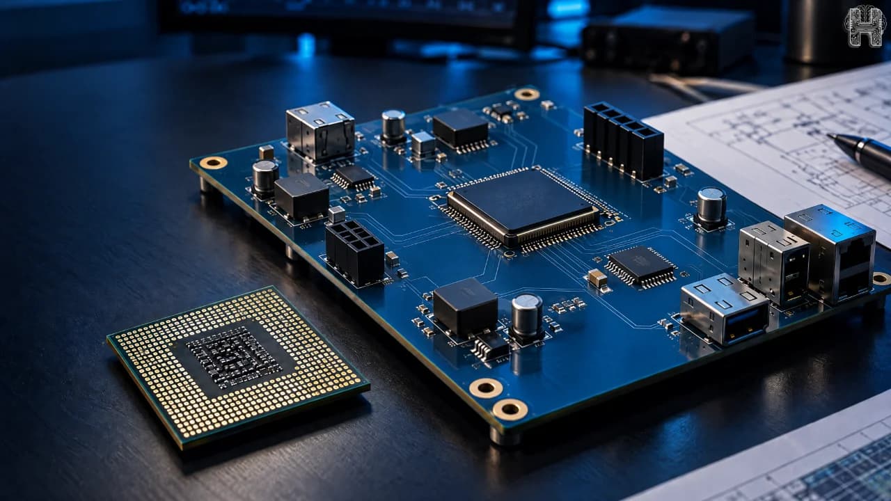
Chip design sits at the heart of nearly every piece of modern technology, from smartphones to AI accelerators. As demand for faster, smaller, and more power-efficient chips grows, engineers face an increasingly complex set of chip design challenges. Understanding these obstacles and how to solve them is essential for any team working in semiconductor chip design today.
What Is the Chip Design Process?
The chip design process involves multiple stages: architecture planning, RTL coding, verification, synthesis, physical design, and final tape-out. Each phase in IC design (integrated circuit design) introduces its own risks, and a misstep at any stage can lead to costly respins. As node sizes shrink and chip complexity increases, integrated circuit design teams must navigate tighter timing budgets, higher power density, and stricter manufacturability rules than ever before.
Common Problems in Chip Design
Understanding the most frequent chip design problems helps teams plan better and avoid delays. Some of the most persistent challenges in chip design include: 1. Power consumption and thermal management- As transistor density increases, managing heat dissipation without sacrificing performance becomes difficult. 2. Timing closure - Meeting timing constraints across millions of gates at advanced nodes is one of the most time-consuming parts of semiconductor design challenges. 3. Signal integrity issues- Crosstalk, noise, and electro-magnetic interference can degrade chip performance if not addressed early. 4. Verification complexity- As designs grow, ensuring functional correctness across every possible state becomes a massive engineering effort. 5. Design for manufacturability (DFM)- A design that works in simulation may still fail during fabrication due to process variability. 6. Yield optimization- Low yield rates directly impact cost and time-to-market, making this one of the most business-critical IC design challenges.
How to Solve Chip Design Challenges
Knowing how to solve chip design challenges requires a combination of smarter tools, better processes, and early-stage planning. Here are proven strategies: 1. Adopt Electronic Design Automation (EDA) Tools Modern electronic design automation platforms help automate synthesis, verification, and layout, significantly reducing human error and turnaround time. Investing in reliable EDA software is one of the most effective ways to address semiconductor design challenges at scale. 2. Leverage Chip Design Automation Chip design automation including AI-assisted floorplanning and automated timing optimization helps teams handle complexity that manual design simply can't manage anymore. This is especially valuable for large SoCs with billions of transistors. 3. Integrate AI Chip Design Techniques AI chip design is transforming how engineers approach layout optimization, power modeling, and verification. Machine learning models can now predict timing violations and thermal hotspots before physical design even begins, cutting down design iteration cycles dramatically. 4. Shift Verification Left Catching bugs early during RTL design rather than post-silicon reduces respin costs. Formal verification and simulation-based testing should be integrated from day one, not treated as an afterthought. 5. Plan for Manufacturability Early Involving foundry partners during the design phase rather than after tape-out helps prevent DFM-related failures and improves yield, directly addressing IC design problems and solutions before they become expensive fixes.
Overcoming Semiconductor Design Challenges for the Future
Overcoming semiconductor design challenges isn't about eliminating complexity it's about managing it intelligently. As chips continue scaling toward smaller nodes and higher performance demands, the combination of automation, AI-driven insights, and disciplined engineering practices will define which teams succeed. At Helektron, we help engineering teams navigate the modern chip design process with smarter tools and deeper insights because solving today's toughest chip design problems requires more than just experience; it requires the right technology partner.
How Helektron.ai Fits Into Modern Design Workflows
Helektron.ai focuses on making electronic design more accessible through AI-assisted circuit and PCB development. Its browser-based workflow helps users move from circuit ideas toward schematic and PCB development without requiring traditional desktop installation. For engineers, students, and electronics enthusiasts exploring AI-assisted design, tools such as Helektron.ai represent how modern chip design, circuit design, and electronic design automation workflows are evolving. For further details contact Team Helektron at +91 87965 06854 Read about- How Does Chip Redesign Work? Understanding the Chip Redesign Process Or visit website- Helektron.ai