Signal Integrity in PCB Design: Causes, Problems and Solutions
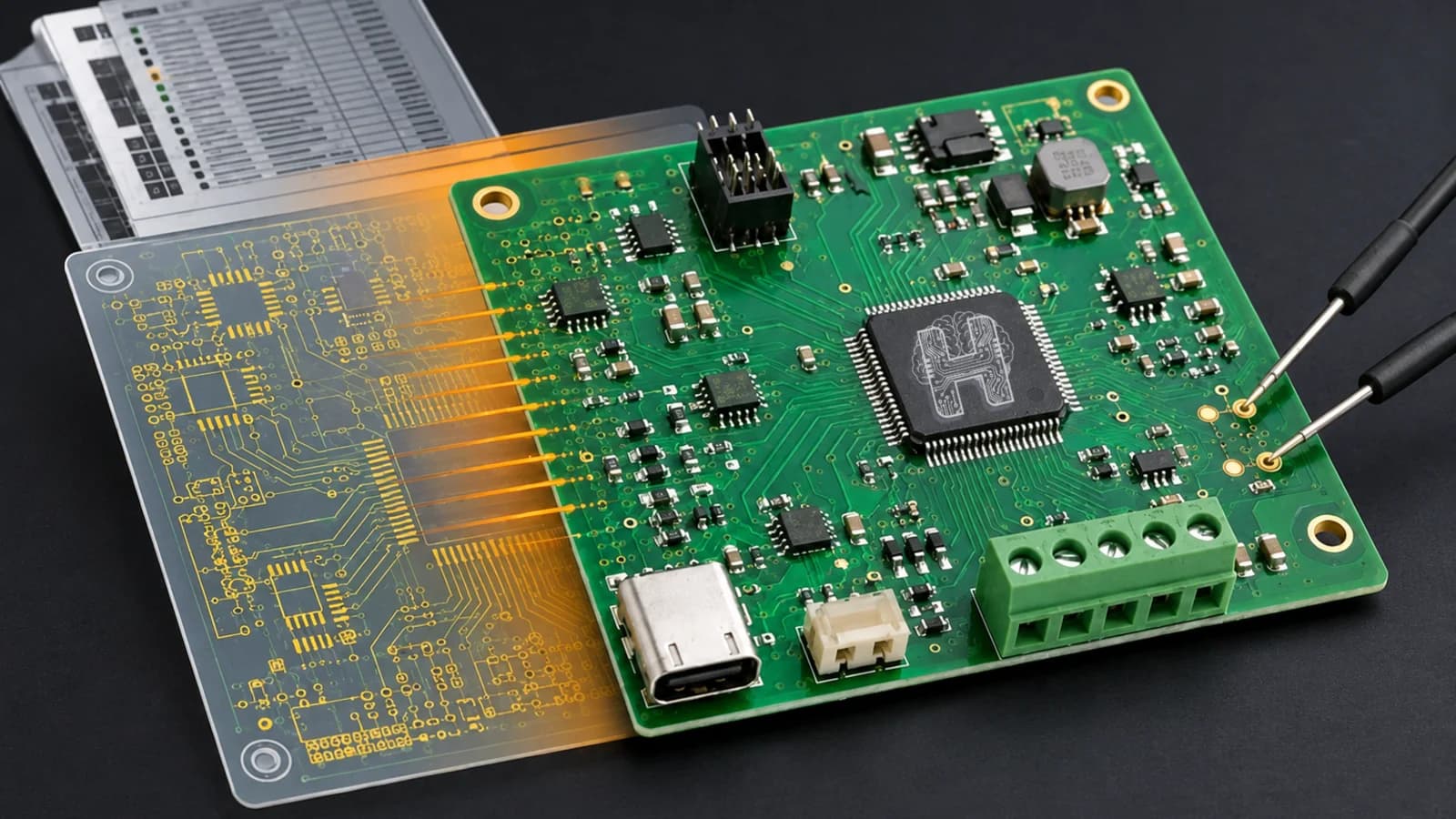
Signal integrity in PCB design is a signal’s ability to travel from driver to receiver without distortion. Most failures come from impedance mismatch, crosstalk and poor return paths. helektron.ai uses AI-powered PCB design checks to catch them before fabrication.
What Is Signal Integrity in PCB Design?
PCB signal integrity describes how accurately electrical signals maintain their intended shape, timing, and voltage while travelling through circuit traces and components. Good signal integrity ensures that electronic devices receive and process signals correctly.
In high-speed PCB design, signals can experience reflections, crosstalk, electromagnetic interference (EMI), and timing issues. These effects can lead to unreliable communication, data errors, and unexpected circuit behaviour.
Therefore, signal integrity is an important consideration throughout the PCB design process, from schematic development to PCB layout optimization.
What Causes Signal Integrity Problems?
Several factors can create signal integrity issues in PCB designs. Some of the most common causes include:
- Impedance mismatch: Differences in impedance between connected traces and components can cause signal reflections.
- Crosstalk: Signals travelling through nearby PCB traces can interfere with one another.
- Poor PCB routing: Incorrect trace placement, excessive lengths, and unsuitable routing paths can affect signal quality.
- Electromagnetic interference: External or internal electromagnetic noise can disturb electrical signals.
- Improper grounding: Poor ground connections and return paths can introduce noise and instability.
Identifying these signal integrity problems early helps reduce PCB design problems and prevents expensive redesigns during manufacturing.
How Can Signal Integrity Be Improved in PCB Design?
Improving signal integrity requires careful planning, accurate routing, and proper design verification. Some effective approaches include:
· Optimize PCB routing: Keep high-speed signal paths short and avoid unnecessary bends.
· Maintain controlled impedance: Match trace impedance with the connected components and transmission lines.
· Use proper grounding: Provide continuous ground planes and reliable return paths.
· Reduce interference: Maintain sufficient spacing between sensitive signal traces.
· Verify the design: Check routing, connectivity, and design constraints before manufacturing.
Following these practices helps improve signal integrity and supports more reliable electronic products.
How AI Is Transforming Signal Integrity and PCB Design
Traditional PCB design involves multiple manual steps, including schematic creation, component selection, routing, and design verification. AI-powered PCB design is changing this workflow by helping engineers simplify circuit development and improve design efficiency.
With AI-assisted circuit design, users can describe their requirements and develop electronic designs more efficiently. AI can also support PCB design optimization by helping users organize design workflows and identify potential issues.
However, AI-assisted design does not automatically guarantee signal integrity. Detailed signal integrity analysis may still require specialized signal integrity analysis tools and simulation techniques, particularly for complex, high-speed circuits.
Signal Integrity Analysis with helektron.ai
This is where helektron ai helps. Helektron is built around AI-assisted circuit design, giving engineers a faster path from concept to a reliable board. Instead of discovering problems during bring-up, you get early feedback while the design is still flexible.
With helektron.ai, you can:
- Automate design verification: automated PCB design verification flags risky nets, impedance discontinuities and layout patterns linked to crosstalk or reflections.
- Speed up PCB layout optimization: AI-driven suggestions support PCB design optimization, from trace spacing to stackup choices.
- Combine circuit design and simulation: review circuit behavior alongside layout decisions rather than in separate steps.
- Reduce rework: early signal integrity analysis cuts the number of prototype spins.
Traditional signal integrity analysis tools are powerful but often steep to learn, and they sit apart from everyday design work. Helektron brings the same thinking into a modern electronic design automation (EDA) workflow, so beginners and experienced engineers can both apply sound practice without becoming simulation specialists.
For further details contact Team Helektron at +91 87965 06854
Read- Best Browser-Based PCB Design Software in 2026
Create you circuit now by clicking directly on- chat.helektron.ai
Visit website- Helektron.ai
Frequently asked questions
What causes signal integrity problems?
Common causes include impedance mismatch, crosstalk, poor PCB routing, electromagnetic interference, and improper grounding.
How can signal integrity be improved?
Signal integrity can be improved through controlled impedance routing, proper grounding, optimized trace spacing, shorter signal paths, and appropriate design verification.
Can AI help with PCB design optimization?
Yes. AI-assisted circuit design can simplify design workflows, support circuit development, and help users work more efficiently. However, specialized signal integrity analysis and verification remain important for complex PCB designs.