What is EDA Automation and Why Does It Matter?
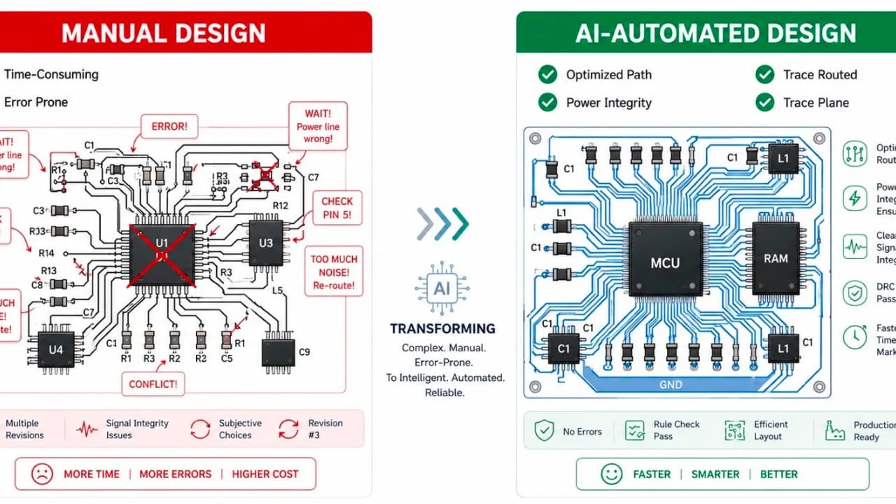
Modern electronics are becoming more complex every year, and manual design processes simply can't keep pace. This is where EDA automation comes in. But what is EDA automation, and why is it reshaping the future of chip and circuit design?
What is EDA Automation?
EDA automation refers to the use of software and intelligent algorithms to automate tasks within electronic design automation the process engineers use to design, simulate, and verify electronic circuits and semiconductor chips. Instead of manually calculating every trace, placement, or connection, EDA tools handle repetitive and complex tasks, allowing engineers to focus on architecture and innovation. Today's electronic design automation software covers the entire design lifecycle, including schematic capture tools, floor planning automation, routing automation, and simulation and verification tools all working together to streamline how circuits move from concept to production.
How AI Is Transforming EDA?
The rise of AI EDA automation has taken traditional EDA software to the next level. AI-powered EDA tools now use machine learning in chip design to predict issues, optimize layouts, and reduce human error before physical testing even begins. With AI-driven EDA platforms, engineers can automate:
- Automated PCB layout and component placement
- Signal integrity analysis to catch issues early
- Design rule checking (DRC) in real time
- Chip design automation for faster semiconductor development
- Circuit design automation across dense, multi-layer boards
This shift toward semiconductor design automation and chip design software means fewer manual errors, faster iterations, and significantly reduced time-to-market.
Why EDA Automation Matters?
As boards get denser and chips more complex, engineers face constant pressure to deliver reliable designs faster. PCB design automation and EDA automation tools solve this by:
- Saving Time - Automating repetitive tasks like floorplanning and routing cuts design time dramatically.
- Improving Accuracy- AI continuously learns from past designs, reducing costly mistakes before manufacturing.
- Boosting Performance- Automated optimization improves signal integrity, thermal efficiency, and power management.
- Enabling Innovation- With routine tasks automated, engineers can focus on strategic design decisions rather than manual troubleshooting.
This is why more engineering teams are searching for the best AI EDA tool for engineers that combines automation with intelligence, not just speed.
Helektron EDA Automation: Built for the Future
At Helektron.ai, we've built an AI-driven EDA platform designed specifically for the challenges engineers face today. Our platform brings together AI-powered EDA tools, intelligent PCB design automation, and integrated simulation and verification tools into one seamless workflow. Whether you're a student, a design engineer, or an enterprise team, Helektron circuit design tools help you move from concept to manufacturing faster without compromising on precision or control.
For further Details contact Team Helektron at +91 87965 06854 This growing shift toward intelligent automation is exactly why Helektron introduced Nexus: The Frontier Industrial AI Reasoning Model built to bring advanced reasoning and decision-making directly into the EDA automation workflow. Or visit website helektron.ai