Electronic Design Automation (EDA): How AI Is Transforming Electronic Design
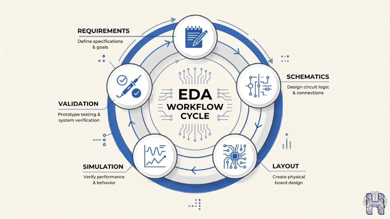
Electronic design automation, or EDA, is the backbone of how modern circuits, PCBs, and electronic products come to life. From schematic design to PCB manufacturing, EDA software guides engineers through every stage of building hardware. Today, AI in electronic design is reshaping that process making circuit design faster, smarter, and accessible to far more people than ever before.
What Is Electronic Design Automation (EDA)?
Electronic Design Automation (EDA) is the use of software tools to design and develop electronic circuits and systems. EDA software allows designers to create circuit schematics, simulate how a circuit behaves, develop a PCB board, identify design problems, and prepare files required for PCB manufacturing. Traditional EDA platforms such as KiCad provide powerful tools for schematic capture and PCB layout. However, many processes still require users to have technical knowledge and perform several steps manually. AI is now helping simplify these workflows by providing intelligent assistance throughout the design process.
How Does Electronic Design Automation Work?
The EDA process generally unfolds across a series of connected stages, and precision at each step matters, since a single mistake in a circuit or PCB design can lead to expensive rework later on:
- Defining requirements- outlining what the circuit needs to accomplish, including power needs and overall function.
- Schematic design- mapping out how each component connects, creating a visual blueprint of the circuit's logic.
- PCB board layout- arranging components on a PCB board and routing traces while avoiding interference.
- Simulation- testing the design virtually to catch electrical issues or mismatches before they cause failures.
- Export and validation- checking the design against standards and exporting files ready for PCB manufacturing.
Why Is Electronic Design Automation Important?
Electronic design automation plays an increasingly critical role in how hardware gets built, and its importance continues to grow as electronic products become more advanced:
- Reduces human error- automating repetitive tasks cuts down on mistakes common in manual circuit and PCB design.
- Speeds up prototyping- engineers move from concept to a testable design far faster than manual methods allow.
- Ensures manufacturing readiness- automated checks confirm a design meets standards required for reliable PCB manufacturing.
- Supports scalability- as products grow more intricate, EDA software helps manage that complexity efficiently.
- Powers modern industries- most connected products today, from IoT to robotics, were shaped by electronic design automation.
What Are the Limitations of Traditional EDA Tools?
Despite everything they offer, traditional EDA tools still come with real limitations that continue to hold back accessibility:
- Steep learning curve- tools like KiCad offer professional-grade depth, but new users often need weeks or months to design confidently.
- Manual component selection- engineers usually research and choose components by hand, which slows the design cycle.
- Time-intensive layout work- PCB board routing still happens largely by hand, demanding careful attention to avoid interference.
- High barrier to entry- the technical depth required makes these tools difficult for students and early-stage founders.
- Limited accessibility- built primarily for experienced engineers, these platforms cause many newcomers to abandon projects.
How AI Is Transforming Electronic Design
AI-assisted electronic design is beginning to close that gap. Instead of manually building a schematic from scratch, AI PCB design tools now let users describe a circuit in plain language and receive an optimized design within minutes. AI-assisted circuit design automates repetitive tasks like component selection and layout suggestions, while automated electronic design workflows help catch errors early, before they turn into costly PCB manufacturing mistakes. This shift is steadily lowering the barrier to entry across the electronics industry.
How Helektron.ai Is Simplifying AI-Powered Electronic Design
Helektron.ai brings this shift to life as an AI PCB design platform built for accessibility. By turning natural-language descriptions into complete schematic and PCB designs, Helektron strips away much of the complexity found in traditional EDA software. Users can generate optimized circuits, understand the components involved, and export manufacturing-ready files, without needing a deep electronics background. As AI in electronic design matures, platforms like Helektron.ai are making professional-grade circuit design available to students, makers, and hardware startups alike.
For further Details contact Team Helektron at +91 87965 06854 Read more about: What Is AI Circuit Design? How AI Simplifies Electronic Design Or visit website helektron.ai