What Is Chip Design and How Does It Connect to PCB Design?
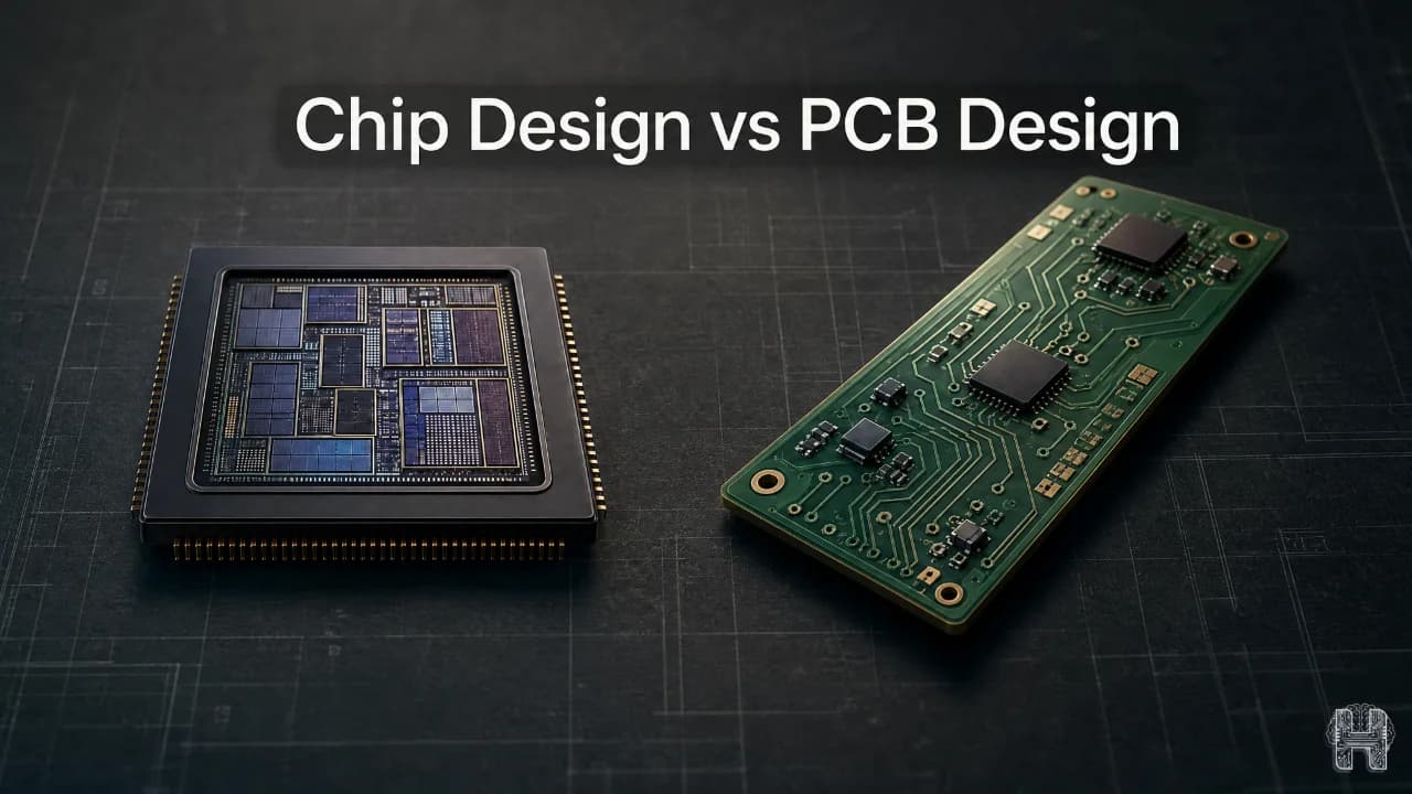
Every electronic product you touch your phone, your laptop, your smartwatch relies on two design worlds working together: chip design and PCB design. Understanding how these two fields connect is essential for engineers, students, and anyone exploring electronic design automation(EDA).
Modern electronic products depend on multiple stages of design, from creating the semiconductor chips that process information to building the physical circuit boards that connect and support those components. Chip design and PCB design are two essential parts of this ecosystem, but they serve very different purposes.
What Is Chip Design?
Chip design is the process of designing an integrated circuit (IC) or semiconductor chip that performs specific electronic functions. A chip may be designed to process data, store information, control devices, manage power, or perform many other tasks. The chip design process generally involves defining the required functionality, creating the circuit architecture, designing logic and physical layouts, verifying performance, and preparing the design for semiconductor manufacturing. Modern electronic design automation tools play an important role in helping engineers manage these complex stages. Different types of chips include microprocessors, memory chips, sensors, ASICs, and system-on-chip devices. As designs become more complex, technologies such as AI chip design are also being explored to help engineers optimize and automate parts of the development workflow.
What Is PCB Design?
PCB design, or pcb board design, is the process of laying out electronic components on a board and connecting them with conductive traces. This is where chips, resistors, capacitors, and connectors come together to form a functioning circuit. Circuit board design focuses on schematic capture, component placement, trace routing, and ensuring signal integrity across the board.
The Chip Design Process
The chip design process typically includes these key stages:
- Specification – define what the chip needs to do
- Architecture and RTL design – describe the chip logic in a hardware description language
- Verification – simulate the design to catch errors early
- Physical design – placing and routing transistors on the die
- Fabrication – manufacturing the chip at a semiconductor foundry
Each stage requires precision, since even a small error can make a chip unusable once fabricated.
Chip Design vs PCB Design: What Is the Difference?
The main difference in chip design vs PCB design is the level at which each technology operates. Chip design focuses on creating the internal electronic circuits of a semiconductor device. PCB design focuses on arranging and connecting electronic components, including those chips, on a physical circuit board. Both processes require accuracy, testing, and specialized design tools. However, PCB designers typically work with already manufactured electronic components, while chip designers create the underlying integrated circuits themselves.
How AI Is Changing Electronic Design
Artificial intelligence is beginning to influence multiple areas of electronics development. AI-powered electronic design can help automate repetitive tasks, analyze design data, and support engineers during complex workflows. Technologies such as AI circuit design and AI PCB design are making electronics design more accessible and efficient. While AI does not replace engineering knowledge, it can assist users in moving faster from an initial idea to a circuit schematic and PCB layout. Platforms such as Helektron.ai are part of this growing shift toward intelligent and accessible electronics design. By helping users explore circuit concepts and PCB workflows, AI-powered tools can support a smoother path from an idea toward a practical electronic design.
How Helektron.ai Connects Chip Design and PCB Design
While chip design focuses on creating the integrated circuits that power modern electronic devices, PCB design brings these components together into a complete and functional electronic system. This is where Helektron.ai fits into the broader electronics design workflow. Helektron.ai helps simplify the journey from an initial circuit idea to schematic creation and PCB design through AI-powered tools. Although chip design and PCB design are different stages of electronics development, both depend on accurate circuit planning, efficient design workflows, and intelligent automation. With the growing role of AI-powered electronic design, AI circuit design, and AI PCB design, Helektron.ai aims to make circuit and PCB development more accessible for students, makers, and engineers. By simplifying complex design processes, Helektron.ai helps users move closer to turning electronic ideas into practical designs.
For further Details contact Team Helektron at +91 87965 06854 Read: Chip Design Rework: The Hidden Cost Killer in Semiconductor Manufacturing Or visit website helektron.ai