What Is Design-for-Manufacturing (DFM) and Why It Matters
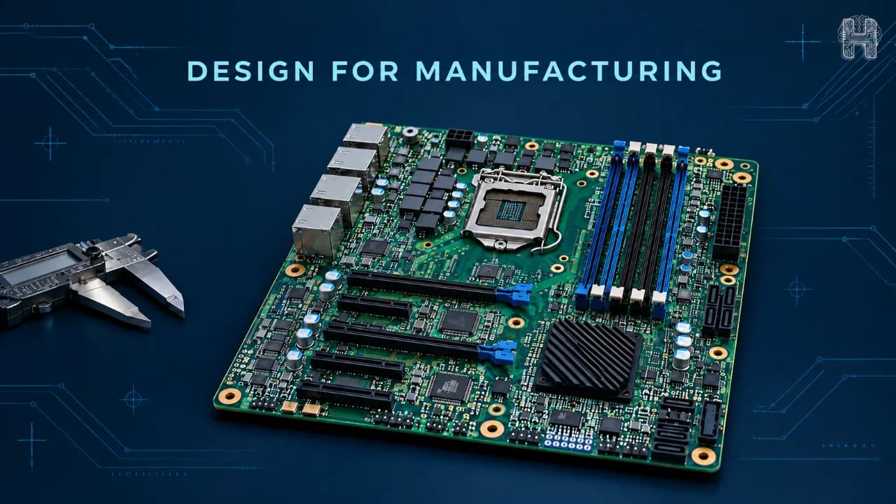
Designing an electronic product is not only about creating a circuit that works. The design must also be practical to manufacture, assemble, test, and scale. DFM is a design approach that helps engineers create products that are easier, more reliable, and more cost-effective to manufacture. For PCB projects, DFM connects the design stage with the PCB manufacturing process, helping identify potential production issues before a board reaches the factory.
What Is Design for Manufacturing (DFM)?
Design for Manufacturing (DFM), also called design for manufacturability, is the process of optimizing a product design so it can be manufactured efficiently and consistently. In electronics, DFM considers factors such as component placement, trace widths, clearances, drill sizes, board dimensions, and assembly requirements. Following appropriate DFM guidelines early can reduce manufacturing errors, redesigns, production delays, and unnecessary costs. For PCB development, this approach is commonly known as DFM in PCB design or PCB DFM.
Why Is DFM Important in PCB design?
DFM important in PCB design because even a small oversight like a trace too thin or a via too close to the board edge can cause manufacturing failures, yield loss, or expensive redesigns. Applying DFM guidelines early helps teams:
- Reduce production costs and scrap rates
- Shorten time-to-market
- Improve product reliability and yield
- Avoid last-minute engineering changes
- Ensure compatibility with manufacturing equipment and processes
For hardware startups and PCB designers alike, skipping DFM often means paying for mistakes later through delayed shipments or failed boards. How Does DFM Works? It typically follows a structured DFM analysis process:
- Design review- Engineers check the layout against standard PCB design rules.
- Rule-based validation- Software tools flag violations of PCB manufacturing design rules, such as minimum trace width or spacing.
- Manufacturer feedback loop- Fabrication partners review the design and suggest adjustments.
- Iteration- Designers refine the board until it passes all manufacturability checks.
This is where an AI builder can significantly speed things up automating rule-checking and flagging design risks in real time, rather than relying solely on manual review cycles.
How to Design a PCB for Manufacturing
If you're wondering how to design a PCB for manufacturing, start with these PCB DFM best practices:
- Follow standard PCB design for manufacturing guidelines for trace width, spacing, and via placement
- Choose materials and finishes your fabricator supports
- Maintain consistent copper weights and layer stack-ups
- Avoid acute-angle traces and overly dense component placement
- Run DFM analysis tools before finalizing your design
How Helektron.ai Supports PCB Design Workflow
Modern tools are making electronics development more accessible. An AI builder such as Helektron.ai can help users move from circuit ideas toward structured electronic designs while reducing some of the manual effort involved in the early design workflow. By combining AI-assisted circuit design with established DFM best practices, engineers, students, and electronics enthusiasts can think about manufacturability earlier instead of treating it as a final-stage consideration. DFM is about creating designs that are not only electrically functional but also practical to manufacture. Incorporating DFM guidelines into the PCB workflow can help create a smoother path from circuit concept to a manufacturable electronic product. For further Details contact Team Helektron at +91 87965 06854 Read about- How to Use AI for Automated PCB Design Rule Checking Or visit website- Helektron.ai