Electrical Rule Check (ERC) in PCB Design: How It Works and Why It Matters
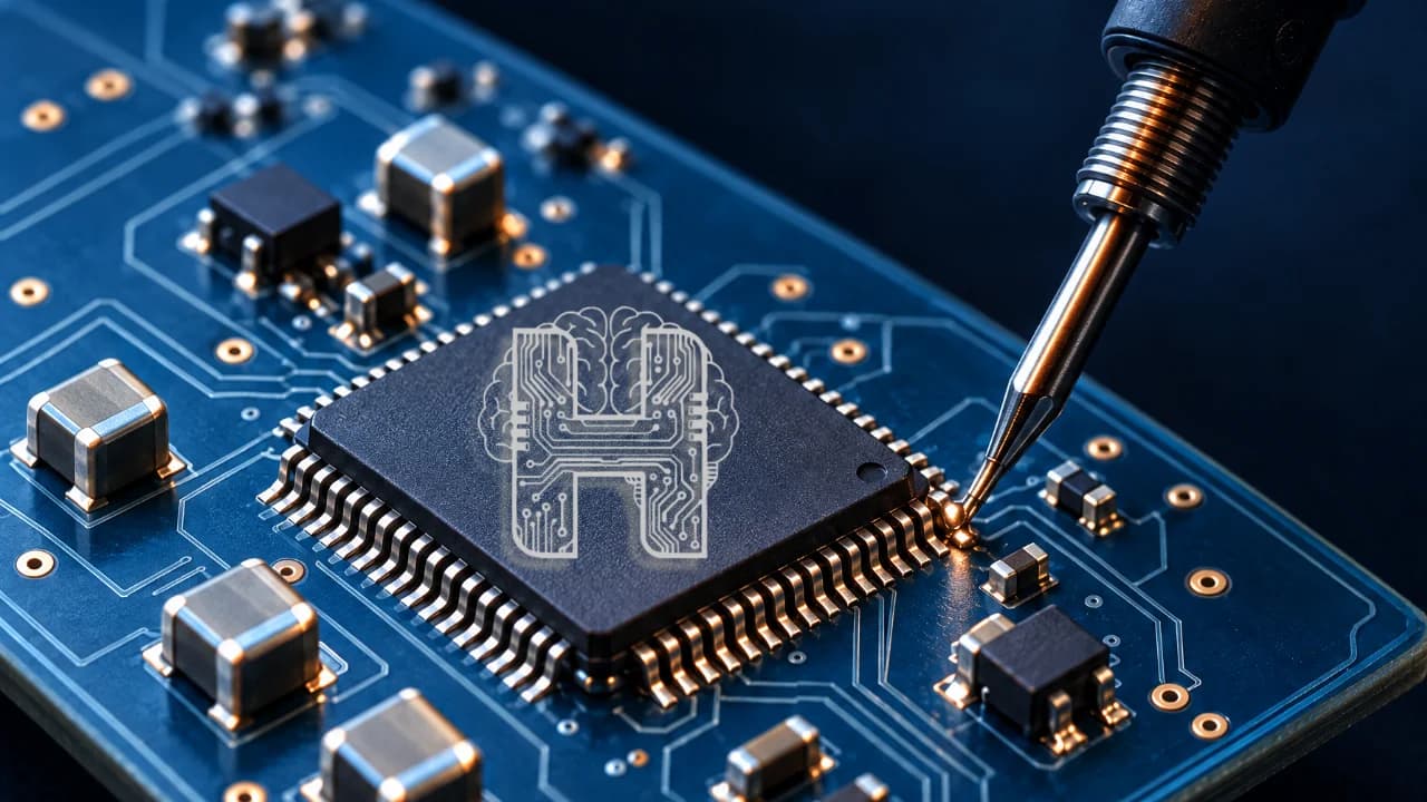
Designing a printed circuit board involves much more than placing components and connecting wires. Before a circuit moves from Schematic Design to PCB Layout, its electrical connections need to be reviewed carefully. Even a small mistake in a schematic can lead to unexpected circuit behavior, debugging problems, or costly redesigns.
ERC is an automated verification process that examines a PCB Schematic for potential electrical problems based on predefined design rules. It helps designers identify issues before they move further into the PCB development process.For beginners learning PCB Design and experienced engineers working on complex Circuit Design, understanding ERC can make the overall design workflow more structured and reliable.
What Is Electrical Rule Check (ERC)?
Electrical Rule Check (ERC) is a schematic verification process used to identify potential electrical rule violations in a circuit design. In simple terms, ERC checks whether the electrical connections in a schematic make sense according to the rules defined by the PCB design software. It examines relationships between components, pins, signals, power connections, and nets. For example, a designer may accidentally leave a required connection incomplete or connect two pins with incompatible electrical characteristics. Such problems can be difficult to notice when reviewing a large schematic manually. An automated Electrical Rule Check PCB process can highlight these potential issues and give the designer an opportunity to investigate them before continuing with the design.
What Is ERC in PCB?
ERC in PCB is important to understand that ERC is primarily associated with the schematic rather than the physical PCB layout. ERC evaluates the electrical logic and connectivity represented in the schematic. It can check whether pins are connected appropriately, whether power-related connections are properly defined and whether certain electrical relationships violate the configured rules. This makes ERC an important step for creating a schematic and developing the physical board. A typical workflow can look like: Circuit Idea → Schematic Design → ERC → PCB Layout → DRC → Manufacturing Running ERC before PCB layout can help reduce the number of electrical problems that reach later stages of development.
How Electrical Rule Check Works
Understanding How Electrical Rule Check works starts with the schematic. When an ERC check is initiated, the EDA software analyzes the components, pins, nets, and electrical properties within the design. The software compares these relationships against its configured PCB Design Rules and reports potential violations. Depending on the software and configuration, ERC may identify issues such as:
- Floating pins
- Unconnected pins
- Unexpected electrical connections
- Power-related connection problems
- Conflicting outputs
- Incorrect pin-type relationships
- Missing or incomplete connections
- Other Electrical rules check schematic violations
The results are generally presented as warnings or errors that the designer can inspect individually. An important point is that an ERC warning does not automatically mean the circuit is incorrect. Some connections may be intentionally designed in a particular way. Engineers should therefore review each reported issue and determine whether it requires correction or can be safely ignored.
Why ERC Is Important in PCB Design
Why ERC is important in PCB design and why it matters becomes clearer when considering how many connections a modern circuit can contain. A simple schematic may have dozens of components and connections, while a complex electronic system can contain thousands of electrical relationships. Manually checking every connection becomes increasingly difficult as the design grows. ERC provides an automated layer of PCB design verification that can help designers identify potential problems earlier. Finding an issue during schematic development is generally more convenient than discovering it after PCB layout, prototyping, or manufacturing. ERC can help designers:
- Detect potential electrical connection problems early
- Reduce manual schematic checking
- Improve schematic quality
- Identify missing or unintended connections
- Catch power-related issues
- Reduce avoidable redesigns
- Support a more structured PCB development workflow
ERC is also useful for beginners because it provides feedback about how components and electrical connections interact. Instead of relying entirely on visual inspection, designers can use ERC results to understand potential weaknesses in their schematic. For professional engineers, ERC becomes even more valuable as circuit complexity increases. It can act as an additional verification layer alongside engineering review, simulation, testing, and other validation methods. However, ERC should not be treated as a replacement for engineering judgment. A schematic can pass an ERC check and still contain a functional or design-level problem that the rules do not detect.
ERC vs DRC in PCB Design
ERC vs DRC in PCB design is an important distinction for anyone learning PCB development. Electrical Rule Check (ERC) primarily focuses on electrical relationships within the schematic, while Design Rule Check (DRC) focuses mainly on physical and layout-related rules. For example:
- ERC checks electrical connectivity and schematic relationships.
- DRC checks physical PCB layout constraints.
- ERC is mainly associated with Schematic Design verification.
- DRC is mainly associated with PCB Layout verification.
- ERC may identify a problematic power connection.
- DRC may identify insufficient spacing between PCB traces or other layout violations.
Both checks serve different purposes, and using them together creates a stronger PCB design verification process.
How Helektron.ai Supports AI-Powered PCB Design
Helektron.ai brings AI into the PCB design process through a browser-based approach, allowing users to work on electronic designs without requiring traditional desktop installation. Helektron AI is designed to make Circuit Design and PCB development more accessible for engineers, students, hobbyists, and beginners. A useful design process also needs verification stages that help users review what has been created. Within this process, ERC can act as an important checkpoint between schematic creation and physical PCB development. This combination of AI-assisted design and structured verification can help make PCB development more efficient while keeping electrical validation part of the workflow. Also read - How Helektron Works: Complete Guide to AI-Powered PCB Design For further details contact Team Helektron at +91 87965 06854 Visit website- Helektron.ai